- 您现在的位置:买卖IC网 > Sheet目录484 > NOIL1SE3000A-GDC (ON Semiconductor)IC IMAGE SENSOR 3MP 369-PGA
NOIL1SN3000A
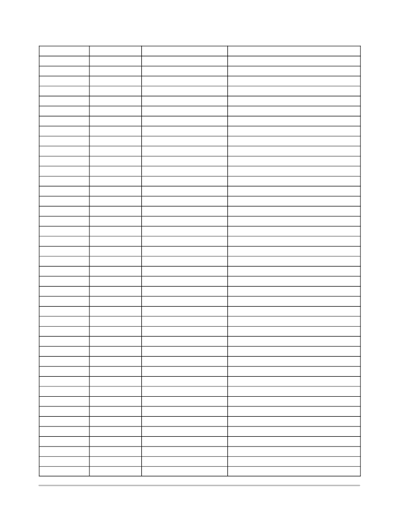
Table 51. PIN LIST
Finger Number
82
83
84
85
86
87
88
89
90
91
92
93
94
95
96
97
98
99
100
101
102
103
104
105
106
107
108
109
110
111
112
113
114
115
116
117
118
119
120
121
122
123
Pin Number
V1
W1
W2
W3
W4
W5
W6
V5
U5
V6
U6
T6
T7
V7
U7
W7
W8
V8
U8
T8
W9
V9
U9
T9
W10
V10
U10
T10
W11
V11
U11
T11
T12
U12
V12
W12
W13
V13
U13
T13
T14
U14
Function
Syncn
Vdd_hs
GNDd_hs
GNDd_hs
Vdd_hs
Vcm
Vdark
GNDadc
Vadc
GNDd
Vdd
GNDadc
Vadc
GNDadc
Vadc
GNDd
Vdd
GNDaa
GNDaa
GNDaa
Vaa
Vaa
GNDaa
GNDaa
Vaa
Vaa
GNDaa
Vaa
Vpix
GNDd
Vdd
Not Assigned
Not Assigned
Reset_n
Exposure 1
Exposure 2
ROT
FOT
Not Assigned
Current_Ref_1
Not Assigned
Analog_Out
Description
LVDS sync channel
2.5-V high speed digital
Ground high speed digital
Ground high speed digital
2.5-V high speed digital
Decoupling analog reference voltage
Decoupling analog reference voltage
Ground ADC
2.5-V ADC
Ground digital
2.5-V digital
Ground ADC
2.5-V ADC
Ground ADC
2.5-V ADC
Ground digital
2.5-V digital
Ground analog
Ground analog
Ground analog
2.5-V analog
2.5-V analog
Ground analog
Ground analog
2.5-V analog
2.5-V analog
Ground analog
2.5-V analog
Vpix (typically 2.5 V)
Ground digital
2.5-V digital
Not assigned
Not assigned
Digital input
Digital input
Digital input
Digital output
Digital output
Not assigned
Current reference resistor
Not assigned
Analog output (leave floating)
http://onsemi.com
46
发布紧急采购,3分钟左右您将得到回复。
相关PDF资料
NOIL1SM0300A-WWC
IC IMAGE SENSOR LUPA300 48LLC
NOIL2SC1300A-GDC
IC IMAGE SENSOR LUPA1300 168PGA
NOIV1SE025KA-GDC
IC IMAGE SENSOR 25MP 355PGA
NP100P04PDG-E1-AY
MOSFET P-CH -40V MP-25ZP/TO-263
NP100P04PLG-E1-AY
MOSFET P-CH -40V MP-25ZP/TO-263
NP100P06PDG-E1-AY
MOSFET P-CH -60V MP-25ZP/TO-263
NP100P06PLG-E1-AY
MOSFET P-CH -60V MP-25ZP/TO-263
NP109N04PUJ-E1B-AY
MOSFET N-CH 40V MP-25ZP/TO-263
相关代理商/技术参数
NOIL1SM0300A-QDC
功能描述:IC IMAGE SENSOR LUPA300 48LLC RoHS:是 类别:传感器,转换器 >> 图像,相机 系列:* 标准包装:480 系列:- 象素大小:6.7µm x 6.7µm 有源象素阵列:768H x 488V 每秒帧数:52 电源电压:3.3V 类型:CMOS 成像 封装/外壳:48-QFP 供应商设备封装:48-QFP 包装:托盘 请注意:* 配用:4H2105-ND - HEADBOARD FOR KAC-004014H2104-ND - KIT EVAL FOR KAC-00401 其它名称:4H20954H2095-NDKAC-00401-CBC-LB-A0
NOIL1SM0300A-WWC
功能描述:IC IMAGE SENSOR LUPA300 48LLC RoHS:是 类别:传感器,转换器 >> 图像,相机 系列:LUPA300 标准包装:480 系列:- 象素大小:6.7µm x 6.7µm 有源象素阵列:768H x 488V 每秒帧数:52 电源电压:3.3V 类型:CMOS 成像 封装/外壳:48-QFP 供应商设备封装:48-QFP 包装:托盘 请注意:* 配用:4H2105-ND - HEADBOARD FOR KAC-004014H2104-ND - KIT EVAL FOR KAC-00401 其它名称:4H20954H2095-NDKAC-00401-CBC-LB-A0
NOIL1SM1300AWES
制造商:ON Semiconductor 功能描述:PW/H
NOIL1SM4000A
制造商:ONSEMI 制造商全称:ON Semiconductor 功能描述:LUPA4000: 4 MegaPixel High Speed CMOS Sensor
NOIL1SM4000A-GDC
功能描述:IC IMAGE SENSOR LUPA4000 127PGA RoHS:是 类别:传感器,转换器 >> 图像,相机 系列:* 标准包装:480 系列:- 象素大小:6.7µm x 6.7µm 有源象素阵列:768H x 488V 每秒帧数:52 电源电压:3.3V 类型:CMOS 成像 封装/外壳:48-QFP 供应商设备封装:48-QFP 包装:托盘 请注意:* 配用:4H2105-ND - HEADBOARD FOR KAC-004014H2104-ND - KIT EVAL FOR KAC-00401 其它名称:4H20954H2095-NDKAC-00401-CBC-LB-A0
NOIL1SN3000A-GDC
功能描述:IC IMAGE SENSOR LUPA3000 369PGA RoHS:是 类别:传感器,转换器 >> 图像,相机 系列:* 标准包装:480 系列:- 象素大小:6.7µm x 6.7µm 有源象素阵列:768H x 488V 每秒帧数:52 电源电压:3.3V 类型:CMOS 成像 封装/外壳:48-QFP 供应商设备封装:48-QFP 包装:托盘 请注意:* 配用:4H2105-ND - HEADBOARD FOR KAC-004014H2104-ND - KIT EVAL FOR KAC-00401 其它名称:4H20954H2095-NDKAC-00401-CBC-LB-A0
NOIL2SC1300A-GDC
功能描述:图像传感器和彩色传感器 LUPA1300-2 COLOR PGA168 RoHS:否 制造商:Avago Technologies 类型:Color Sensors 工作电源电压:2.5 V 封装 / 箱体: 图象大小: 颜色读出:Color 最大工作温度:+ 70 C 最小工作温度:- 25 C 封装:Reel
NOIL2SM1300A-GDC
功能描述:IC IMAGE SENSOR LUPA1300 168PGA RoHS:是 类别:传感器,转换器 >> 图像,相机 系列:* 标准包装:480 系列:- 象素大小:6.7µm x 6.7µm 有源象素阵列:768H x 488V 每秒帧数:52 电源电压:3.3V 类型:CMOS 成像 封装/外壳:48-QFP 供应商设备封装:48-QFP 包装:托盘 请注意:* 配用:4H2105-ND - HEADBOARD FOR KAC-004014H2104-ND - KIT EVAL FOR KAC-00401 其它名称:4H20954H2095-NDKAC-00401-CBC-LB-A0
